
A community for the repair bench. Since 2022.LAPTOP + DESKTOP BOARD REPAIR
Advertisement
Service · EC / KBC unlock Unlock MEC17xx, Nuvoton & ITE with a BIOS patch
  • BIOS patch method
  • Private check
  • For verified owners & repair technicians
Chat on WhatsApp +92 328 0493988 · Replies on WhatsApp
Service · Dell BIOS password Dell master BIOS codes from your System Number
  • Suffixes 8FC8 CF1B 3FE2 9ABE 1B58 E7A8
  • Private check
  • For verified owners & repair technicians
Chat on WhatsApp +92 328 0493988 · Replies on WhatsApp

Oppo Oppo Reno 2F Network signal Repair Solution Ways Schematic Diagram pdf

Oppo smart phones schematic diagrames and boardviews
Search files by board code
Browse all 33,242 files →
Oppo Reno 2F Network signal
Repair Solution Ways
Schematic Diagram pdf
 
About this board

This thread is for the Oppo Reno 2F Network signal Repair Solution Ways.

What this thread covers
  • Schematic / circuit diagram (PDF)

Common faults on this board: no power, boot loop, no charging, or no network/baseband after water damage or a bad flash.

Make a full backup first and keep the original firmware; the wrong region file can break network or IMEI.

If you have a working file for this board, please share it below. More files: search Oppo Reno 2F Network signal Repair Solution Ways in File Finder.

Attachments
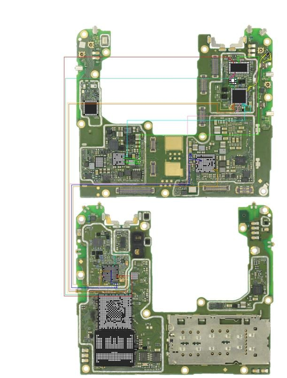
Oppo Reno 2F Network signal Repair Solution Ways Schematic Diagram pdf – 1717916804106

Make PKBIOSFIX part of your bench.

Professional resources. Shared experience. A stronger repair community.

Explore PRO
Back
Top