
A community for the repair bench. Since 2022.LAPTOP + DESKTOP BOARD REPAIR
Advertisement
Service · EC / KBC unlock Unlock MEC17xx, Nuvoton & ITE with a BIOS patch
  • BIOS patch method
  • Private check
  • For verified owners & repair technicians
Chat on WhatsApp +92 328 0493988 · Replies on WhatsApp
Service · Dell BIOS password Dell master BIOS codes from your System Number
  • Suffixes 8FC8 CF1B 3FE2 9ABE 1B58 E7A8
  • Private check
  • For verified owners & repair technicians
Chat on WhatsApp +92 328 0493988 · Replies on WhatsApp

Samsung SAMSUNG Galaxy A13 SM-A137f Schematic Diagram pdf

Samsung smart phones schematic diagrames and boardviews
Search files by board code
Browse all 33,041 files →
SAMSUNG Galaxy A13 SM-A137f Schematic Diagram pdf
 
About this board

Files for the Samsung Galaxy A13 SM-A137f motherboard.

Files listed for this board
  • Schematic / circuit diagram (PDF)

Useful when the phone is dead, restarts in a loop, does not charge, or loses network after a repair.

Before flashing, back up user data and note the IMEI; flashing a file for another region can cause network problems.

Have a tested file for this board? Reply below and help the next technician. Looking for something else? Search all files in the File Finder.

Attachments
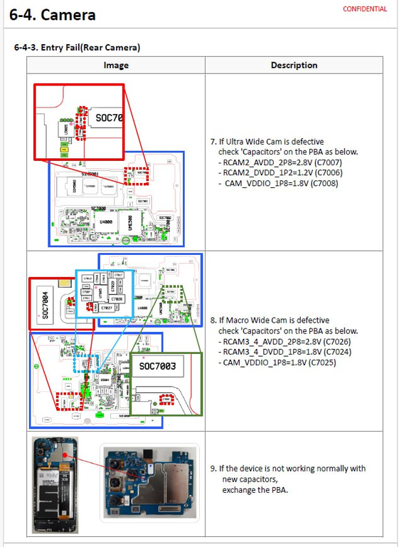
SAMSUNG Galaxy A13  SM-A137f  Schematic Diagram pdf – 1716565413874

Make PKBIOSFIX part of your bench.

Professional resources. Shared experience. A stronger repair community.

Explore PRO
Back
Top